Thin-Films Characterization Lab
Atomic Force Microscope (AFM)
EXPLORER™ Scanning Probe Microscope design , TopoMetrix's Scanning Tip Technology™, a unique feature that permits imaging samples of any diameter, thickness or mass. This TopoMetrix-exclusive design also makes it possible to perform contact, non-contact, lateral force, force modulation and other Atomic Force Microscopy (AFM) techniques without any hardware changes

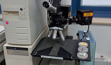
Combined AFM-NSOM
Optical Characterization of Near Field detectors

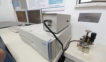
SENTECH SE400 Ellipsometer
Ellipsometry is a very sensitive surface and thin film measuring technique using polarized light (HeNe 632.8 nm) to determine optical properties and thickness.
Measurement parameters can be customized to the sample to maximize data accuracy where the ellipsometric data is content-rich.
Thin Film Applications: Semiconductors, Optical coatings, Dielectrics, Metals, Photovoltaics
![20220608_123454[1].jpg](https://static.wixstatic.com/media/dde8aa_1b4f49b47e43426eaac2f5ea6a093915~mv2.jpg/v1/fill/w_354,h_208,al_c,q_80,usm_0.66_1.00_0.01,enc_avif,quality_auto/20220608_123454%5B1%5D.jpg)
KLA Tencor Prometrix FT-750 Film Thickness Measurement
FT-750 Film Thickness Probe is highly advanced film thickness measurement system designed for in-line inspection and measurement of patterned wafers. With its Pattern Recognition (PR) feature, the FT-750 system enables you to set up and run tests on patterned wafers without having to manually align each wafer or to select test sites on each wafer.

Near Field Scanning Optical Microscope (NSOM)
EXPLORER™ Scanning Probe Microscope
Tencor Alpha Step 200 Profilometer
The Tencor Alphastep 200 Profilometer has a stylus that is placed in direct contact with the wafer surface and is scanned across the surface. Vertical displacement of the stylus is recorded versus the scan distance.

Nanometrics NanoSpec AFT 4000
Table top automated film thickness and reflectivity system. Standard Film Types Measured, Single Layer Films: Visible 500-50,000Å; UV 25-500Å. Double Layer Films: Visible Top Layer 100-30,000Å; Bottom Layer 100-10,000Å. Single Layer Thick Films: Visible 4-75 microns. Reflectance: Visible 400-850nm.